Labels

Showing posts with label Reviews. Show all posts

Internet Explorer 10 Tips and Tricks: It Can Do More Than You Think


When Microsoft unveiled Windows 8, one of the most interesting things about it was the new iteration of Internet Explorer. If viewed via the Start screen, the slimmed-down browser offers maximum space for viewing web pages thanks to the position of buttons and the address bar striped across the bottom of the screen (where people don’t usually read). It’s a fascinating new approach, but Internet Explorer 10 is apparently low on features and options.
In fact, you might think that it can’t do much other than browse the web. Of course, you would be wrong. Thanks to the Desktop view in Windows 8 you can configure both the Metro and traditional “views” of the browser.
This article refers to the new-look Windows 8 as “Metro”, a term popularised by Microsoft and technology journalists to describe the tile-based interface seen in Windows 8 (and preceded on Windows Phone devices). Although this is no longer the name given to the user interface, it is the one that most people are familiar with.

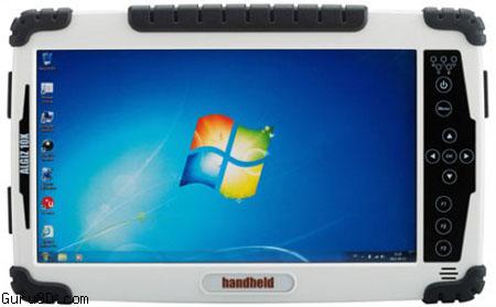
New Amazing handheld windows tablet PC


The Handheld Group is ready to release the Algiz 10x 10.1-inch rugged tablet PC. Designed for field professionals, this rugged tablet PC is IP65-rated and meets stringent MIL-STD-810G military standards for protecting against dust, water, vibrations, drops, extreme temperatures and varying altitudes. Weighing at just 1.3 kg (2.9 lbs) and measuring at 32 mm thick, the Algiz 10X is equipped with a 10.1-inch touchscreen display with the latest generation of MaxView technology, a u-blox GPS receiver, WAAS/EGNOS/MSAS capability, Bluetooth 4.0 and WLAN 802.11 b/g/n. Other specs include a 5-megapixel camera with LED flash, USB 2.0, VGA and RS232 ports.
 It also provides an Intel Atom N2800 dual-core processor with a 4GB of DDR3 RAM, a choice of a 64GB or a 128GB SSD, a microSD for storage expansion and the Microsoft Windows 7 Ultimate operating system. The Algiz 10X rugged 10.1-inch Windows tablet PC will be available in January 2013.

New Crysis 3 Multiplayer Introduction Video


n this Crysis 3 video, Producer Mike Read explains some of the new gameplay elements introduced to the Multiplayer of Crysis 3. Tactically adapt to any combat scenario with the stealth and armor abilities of your unique Nanosuit as you battle through the seven wonders of New York's Liberty Dome. Unleash the firepower of your all-new, high-tech bow and alien weaponry to hunt down other players in a variety of Multiplayer game modes, including "Hunter Mode" and "Crash Site".
 Challenge and be challenged by your friends with the NY Feed, and choose your own path towards leaderboard dominance.

Well, i've been a big fan of crytek. Played Every crysis....................Cant wait for Crysis 3 !!!
To Preorder 
CLICK HERE


MSI GeForce GTX 650 Ti


NVIDIA recently released the somewhat entry level GTX 650, but it is performing at Radeon 7700 levels game performance wise. That means that there was a gap left open up-to the Radeon 7800 series. To fill that gap NVIDIA now is releasing one more product, it's the all new  GeForce GTX 650 Ti (with that Tiindicating a distinct  difference).
See the regular GTX 650 comes heavily castrated with just 384 shader cores whereas the Ti model is released with a much better 768 CUDA cores (shader processors) and a 925 MHz GPU clock (for the reference products). So that's nearly double the processing performance. The budget graphics card series for gamers therefore just got a little more interesting. Albeit we say that 150 USD/EUR should not exactly really carry the tag budget.
But if you do not want (or can not)  to spend heaps of money on your HTPC card or simply game in resolutions lower then 1920x1080 then for the 150 bucks the GeForce GTX 650 Ti positions itself smack-down in-between AMD's Radeon HD 7770 and 7850, and that really is a comfortable spot to be in for many of you.
Being based on the Kepler GPU architecture yet  obviously NVIDIA did not want to make yet another separate chip. So The GTX 650 Ti is the same one used on the regular GTX 660, yup the GTX 650 Ti is using the "GF106" silicon opposed to the GK107 being used on the regular 650 model (it's confusing as heck we know).
However that  GK106 silicon is armed with 768 active shader processor cores divided over four processor clusters running at 930 MHz on the reference products. That means that the GeForce GTX 650 Ti packs decent enough punch whilst consuming a relatively small amount of power. Interesting to know is that the 650 series all have a fixed 3D clock, so there is no dynamic boost aka Turbo functionality or anything. Thanks to that it actually overclocks really well you will find out in our AIB/AIC reviews.
The board partners will released two models of the 650 Ti series, one with 1 GB and the other one 2GB of 5GHz GDDR5. The big bad limiter however will be the the memory bus width, it is 128-bit memory and that will have a seriously impact on the overall rendering and compute performance. 
Overall the GeForce GTX 650 Ti, as we'll demonstrate, has enough horsepower to step into the DX11 games at up-to 1600x1200 resolutions, with the somewhat dated titles a resolution of 1920x1080/1200 will actually be playable as well. And if you can forfeit to medium quality settings in a game and don't do any crazy stuff Anti-aliasing wise, it's definitely plausible to play games really nicely at such resolutions versus acceptable framerates.
So in today's review we'll look at the 650 Ti from MSI, in specific the Power Edition. The SKU comes with a customized PCB, the Cyclone II cooler and in fact is factory overclocked towards 993 MHz on the core clock frequency. Have a peek at what is the MSI GeForce GTX 650 Ti power edition offers.

Reference technology and specs

So as always we'll first address the reference technology. A product like tested today is always based of the reference design and sometimes optimized a little in terms of VRM, PCB design, component usage, clock frequencies, cooling and display outputs. But the building template the manufacturers work from is in fact that reference design. 
In this segment of the article we will look at the reference (original design) based specs and architecture. The GeForce GTX 650 Ti is based on the Kepler GPU architecture. The product however is using the GK106 which is based on a 28nm fabrication process. You guys all know the GK106 from the GeForce GTX 660 products. That chip has 2.64 Billion transistors.
The GeForce GTX 650 Ti whould be 40% faster than the GTX 650 on average.
When we peek at NVIDIA's slide decks we see them denoting that the GeForce GTX 650 Ti has been designed for 1080p gaming with medium settings and FXAA. That's true but please do understand this remains a budget level graphics card .
  • The GeForce GTX 650 boasts 384 CUDA (shader) cores (GK107)
  • The GeForce GTX 650 Ti  boasts 768 CUDA (shader) cores (GK106)
  • The GeForce GTX 660 boasts 960 CUDA (shader) cores (GK106)
  • The GeForce GTX 660 Ti boasts 1344 CUDA (shader) cores (GK104)
  • The GeForce GTX 670 boasts 1344 CUDA (shader) cores (GK104)
  • The GeForce GTX 680 boasts 1536 CUDA (shader) cores (GK104)
The GeForce GTX 650 Ti ships with 4 activated SMX units containing 768 CUDA Cores and 64 texture units. The graphics core clock speed of the GeForce GTX 650 Ti is 925 Mhz (reference frequency - AIB/AIC partners will ship with higher clocks) . GPU Boost is not available. The GeForce GTX 650 Ti memory speed is loacked at an 5400MHz effective data rate based on a1350 MHz quad data rate for GDDR5.
 
You'll notice that the TDP of the card is set at maximum of 110 watts, however since a segment of the GPU is not used  the realistic power consumption will be a little lower. We measured that to be roughly 90~100 Watts actually. So the GeForce GTX 650 Ti draws relatively little power. It still ships with an external power connector. This power connector provides additional headroom for overclocking. Many GeForce GTX 650 Ti boards are capable of hitting speeds in excess of 1100 MHz quite easily.
The idle power of GeForce GTX 650 Ti is 5W to 10W representing terrific in class idle power. In addition, HD video playable is ~13W, again representing best in class power consumption.
Display outputs include two dual-link DVIs and one mini-HDMI, however this could be different per board partner.
128-bit Memory Interface
The memory subsystem of the GeForce GTX 650 Ti consists of two 64-bit memory controllers in use (128-bit) with either 1GB or 2GB of GDDR5 memory.
We already mentioned it, another change is the ROP (raster operation) engine, cut down to 16 units opposed to 24 on it's bigger brother the GTX 660. With this release, NVIDIA now has the real mid-range products on its way. The new graphics adapters are of course DirectX 11.1 ready.
With Windows 8, 7 and Vista also being DX11 ready all we need are more new games to take advantage of DirectCompute, multi-threading, hardware tessellation and the latest shader 5.0 extensions. For your reference here's a quick overview of some of the more recent graphics cards.
GeForce GTX
650
GeForce GTX
650 Ti
GeForce GTX
660
GeForce GTX
660 Ti
GeForce GTX
670
GeForce GTX
680
GeForce GTX
690
Stream (Shader) Processors384768 9601344134415363072
Core Clock (MHz)10589259809159151006915
Shader Clock (MHz)1058925-----
Boost clock (Mhz)-103398098010581019
Memory Clock (effective MHz)5000 540060086008600860086008
Memory amount<2048<2048 20482048204820484096
Memory Interface128-bit128-bit 192-bit192-bit256-bit256-bit256-bit
Memory TypeGDDR5GDDR5 GDDR5GDDR5GDDR5GDDR5GDDR5
For Kepler, NVIDIA kept their memory controllers GDDR5 compatible. Memory wise NVIDIA has nice large memory volumes due to their architecture, we pass 2 GB as standard these days for most of NVIDIA's series 600 graphics cards in the high range spectrum. We expect most GTX 650 Ti cards to come with 1 GB of graphics memory in order to remain price competitive, the 2GB models will be roughlt 25 USD/EUR more expensive.


PowerColor Devil13 HD7990


Introduction
Enthusiast based graphics cards, ones that come complete with all the bells and whistles, are usually to be found late in the lifespan of a particular GPU. Today we have a definite switch around of that concept as the PowerColor Devil13 HD7990 has appeared in our offices without much of a fanfare, and certainly without a reference HD7990 being hinted at, much less produced.
It's therefore perfectly possible that this will be the only HD7990 available. Two full-fat HD7970 cores in one card. It reminds us, conceptually, of the ASUS Ares. The Devil13 certainly matches up in terms of ambition and packaging, as well as price.
In some respects we're always nervous about dual-GPU cards. The power requirements and heat issues normally mean that the GPUs are cut-down from the top-end models. However, PowerColor have given us two full on Tahiti XT cores so it will be interesting to see if the card matches up against two solo HD7970s.
We have a lot to cover in this review, so let us crack on.
Technical Specifications
It's a positive beast of a thing. Triple slot cooler, 6GB of GDDR5, 3 8pin PCI-e power connections. It's extreme in every sense. 
Graphics EngineRADEON HD7990
Video Memory6GB GDDR5
Engine Clock925MHz / 1000MHz
Memory Clock1375MHz x 4 (5.5Gbps)
Memory Interface384bit X2
DirectX® Support11.1
Bus StandardPCIE 3.0
Standard Display ConnecorsDL DVI-I / SL DVI-D / HDMI / 2 X mini DisplayPort
OpenGLSupport
CrossFireX™ TechnologySupport
ATI Stream TechnologySupport
ATI Eyefinity TechnologySupport
VGA OutputYes, By DVI to VGA converter
DVI OutputDL-DVI-I/ SL-DVI-D
DisplayPortOn Board(mini DP) x2
HDMIOn Board
HDCP SupportSupport
VGA2048x1536
DVI2560x1600
DisplayPort4096x2160
HDMI4096x2160
Board Dimensions315mmx140mmx60mm
Minimum System Power requirement (W)850W
Extention Power Connectorthree 8-pin PCI Express Power connectors
 Overclocking
We'd expect that the power requirements of the Devil13 are enough to make overclocking a hopeful task at best, yet we managed to overclock both GPUs, and the GDDR5, by 125MHz. Remember that the memory is quad-pumped. This is a hugely surprising result. 12.5% increases aren't something we'd have expected from the card at all.
 PowerColor Devil13 HD7990 Overclocking
Temperatures
There has been much talk about the early batch of Devil13s having a problem with the pressure applied by the cooler leading to increased temperatures. It's exactly why here at OC3D we always wait for the final version of a product before reviewing it so that we see results you can obtain too, and the Devil13 is definitely cool, even with our overclock.
Quiet is subjective, and it's not the quietest card we've ever seen, but it's easily something you can live with and not distracting.
 

Benchmarks

Alien vs Predator
Starting with AvP, the Devil13 lives up to its diabolic moniker by spanking everything else we've tested. The overclock in particular gives huge gains.


MSI FM-2 A85XA-G65 motherboard


The MSI FM2 A85XA-G65 locked and loaded with features

There's a pretty good chance you have just read our A10 series APU review from AMD. These APU's slash processors offer value for money in the entry level PC market. Obviously the APU needs some sort of infrastructure as well, and that's where FM2 motherboards jump in. In the weeks to come you are going to notice a lot of reviews on A85X motherboards from various manufacturers. Now we have multiple of these motherboards in the lab here so for the APu reviews we used ASUS board in this review an MSI board and there will be more. 
But what are these new motherboards all about ? Well, the chip used on these puppies is the FCH and alongside the Trinity processor APUs the new A85X FCH is born.
First off, to clear some confusion, Trinity-based APUs are not socket-compatible with Llano. So the new A10 APU would not fit on the older models motherboards.  The old chipset and the new one however are hard to separate. The A85X FCH gives you eight SATA 6Gb/s-capable ports, RAID 5 support, and the ability to divide the APU’s 16 lanes of PCI Express 2.0 into a pair of x8 links. That really is the big difference right there. Then of course the motherboard manufacturers will add more ICs and designs to make the products more attractive.
MSI for example, offer the board as tested today with "Military Class III" components for prolonged stable power delivery and longevity, albeit most Taiwanese OEMs have already been using solid-state capacitors and high quality chokes for quite some time.

The A85 chipset and Socket FM2

With the launch of Llano alongside came A75 Fusion controller hubs (FCH)‎ based motherboards, with Trinity that would be A85 (or I should really say A85X). The APU's all have an embedded Northbridge, the motherboards do need some sort of a Southbridge for external connectivity and other controllers. This takes the form of the A75/A85X chipset, also known as the Southbridge or FCH. It connects from the APU's PCI-Express 2.0 bus over four links to the chipset. 
New is the A85X series chipsets for FM2 socket processors. It's a little more enthusiast in terms of features.
It is important to understand that most FM2 motherboards will ship with one of two Fusion Controller Hubs (FCH) - either A85X or A75. To add confusion to the mix, A75 can be used with both Llano and Piledriver, so some vendors will be using the A75 FCH but naming their boards as 'A85'. Vendors will be using A85X chipset and also naming their boards as 'A85'. The differences between the two indicate that A85X has eight SATA 6 Gbps ports native compared to six on A75, and that A85X can support RAID 5 operation whereas A75 cannot.
A second difference is that A85X can support 2x8 lane Crossfire. So for A85 up-to eight SATA-600 ports are supported with support for RAID 0, 1 and 10. That is alongside 10 USB 2.0 ports, 2 USB 1.1 ports and yes, USB 3.0 leads native straight out of the A85 chipset as well with four USB 3.0 ports. Obviously the chipset also offers support for the older PCI slot, up-to three of them.
This is all embedded inside the FCH, thus motherboard manufacturers do not have to purchase extra USB 3.0 and SATA controllers, making the bill of materials a chunk smaller and cheaper. An interesting point with Trinity processors is that AMD introduces a new socket FM2.
Otherwise, you’re looking at the same combination of USB 2.0 and 3.0 ports (4 + 10), the same four-lane Unified Media Interface, four lanes of second-gen PCIe, and four-channel audio (along with FIS-based switching, mSATA support, legacy PCI, and so on). AMD has not yet added PCI Express 3.0 support to any of its platforms, and isn’t expected to for some time.
More than likely, you’ll look to A75-based boards with Socket FM2 interfaces to save a little money, or A85-based platforms as a more feature-complete step up.

The Trinity APUs overview

At launch AMD will be releasing six Trinity based APUs with two different TDPs (100/65W). Have a look at the overview below as to what you may expect. 


AMD A10 5800K


Trinity Desktop APUs - the 2nd Generation AMD A-Series

Back in May AMD introduced a series of AMD A10 'Trinity' APUs as mobile and notebook solutions. The new APU series is based on a new architecture that should bring its performance above previously released Llano based products from that same A series.
The new chips came with a codename that you all will recognize, Trinity. Trinity will thus be the successor of the current  AMD A4, A6 and A8 Llano-processors.
First and foremost, we are a bit of an enthusiast based website so I need to make it very clear here, the A10 and A8 APU processors are entry level to mid-range targeted processors. That means you are  looking at reasonable up-to okay CPU performance versus a greatly enhanced integrated GPU, and all that for very interesting prices. Tested today is the A10 5800K APU for example, costing roughly 125 EUR.
Based on the Trinity APU architecture there will be several APU models to be found which we'll place in an overview later on.
Our tested model is the A10-5800K APU is rated at 100W running at 3.8 GHz with a Turbo allowance towards 4200 MHz. The A10 APUs have a 4MB L2 cache and pack 384 Radeon (shader) cores with that embedded GPU running at 800 MHz.
By itself not a massive GPU change opposed to the previous generation which had 400 shader cores however the new AMD graphics architecture is applied and offers a significant leap in performance for integrated graphics alright. Processor wise Trinity is based on Piledriver cores, basically the new 2nd revision of AMD's Bulldozers cores which we all know from AMD's FX series processors.

APU

As you guys have learned by now an APU is a processor series with integrated graphics (in the processor die), an idea much like what Intel did with Sandy Bridge and later on Ivy Bridge processors.
APU is an abbreviation ofan  Accelerated Processing Unit. Back in 2005, when AMD bought ATI, rumors immediately popped up about the technology you will learn about today. Earlier last in 2011 you have noticed the introduction of APUs like the E350 (Zacate and Ontario chips), these however can be seen as 'Atom' like processors for netbooks and entry level notebooks. The Llano series was intended to address the entry-level to mid-range segment of both the notebook, but also desktop market. 
The APU processor reviewed today for example is targeted against Intel's Sandy Bridge Core i5 2300  processors. Now, processor power wise things will be easy, Intel has the upper hand, but the GPU architecture in Trinity is just so much more advanced allowing you to do much more with less components in your PC, especially in the multi-media segment. Llano APUs are going to dominate as that overall experience is much more powerful.
Combine that with a much more advanced motherboard chipset and the new A85 series motherboards, and you'll notice that AMD has a lot more to bring to the table.

Trinity as a package

As explained in the introduction AMD is now applying Trinity technology towards the new APUs. The last generation technology was called Llano, which will remain available for quite a while we think. Trinity is based on the very same 32nm fabrication but the chip is completely new. For the CPU part this APU now comes with what is called piledriver cores, four of them. The Piledriver core is the 2nd generation Bulldozer core which on that end you guys all know from the FX series processors.
For the GPU part of the APU things have changed massively. Trinity has a Radeon GPU with 384 shader cores. The distict difference is that Llano had an architecture based on the Radeon 5000, Trinity makes use of Radeon 6000 architecture which you all know under the northern islands codenames. Also an upgraded model video-encoder has been integrated, based on the latest Radeon 7000 series. AMD calls the GPU embedded into the A10 5800K the Radeon HD 7660D, it runs at 800 MHz.
Trinity comes with a dual-channel memory controller with official support up-to 1866 MHz, new is low voltage memory support which will make the use of 1.25V and 1.5V very easy. Just like Llano Trinity makes use of an integrated PCI_Express 2.0 controller which you can use for a dedicated graphics card. In fact we'll try that out with a GeForce GTX 580 later on in the article.  There are 25 PCIe lanes available of which four are used for the chipset
Trinity will have a slightly higher die-size opposed to the previous generation at 246 mm²with 1.3 Billion transistors. To make a bold comparison, Intel has a 216mm² die on 32nm Sandy bridge processors which have 1.16 Billion transistors. Ivy bridge his 160mm² (22nm) with 1.4 Billion transistors.
 
Trinity APU die 

Trinity Piledriver CPU Cores

We do need to get a littler deeper into the processors cores as thee have been significant changes. The 2nd generation Bulldozer cores are Piledriver, as such  Piledriver cores are used inside the new Trinity APUs. Honestly we have not been very positive about Bulldozer at all as the performance per core simply is not up-to snuff anno 2012.
AMD claims that they have tweaked the logical CPU cores a little to make them perform the way they are intended to be. Inside the APu you'll spot two clusters, or modules fir the CPU side of things. Inside the modules we see two integer CPU-cores which both share a floating point unit. Each module has a 2MB L2 cache. Trinity uses two of these modules which brings it towards four logical processor cores.
Mind you that there will be Trinity versions out with one module disabled, and thus will be 2-core solutions.
That also means that each of the four CPU cores will have 64KB instruction + 64KB data L1 cache per CPU core. Then there's 1MB of L2 cache per CPU core and for Piledriver. There's no shared L3 cache. The processor cores have been tweaked though the average instruction per clock-cycle has improved by a another say 10%
Good news is to see support for AVX, AVX 1.1, FMA3 and AES instructions sets, something Llano missed out on. 
One more improvement for Trinity is AMD Turbo Core 3.0, and the technology has been enhanced. The Turbo mode can clock the processor cores up and down real fast when the power usage and temperature allow for it. The A10-5800K APU tested today can turbo towards 4200 MHz.
So Trinity  has three primary elements merged into the APU; the Northbridge, the CPU and the GPU. Intel places more focus on raw CPU performance, AMD places more focus on the multi-media experience, thus the GPU.
There's a heck of a lot more to be found inside the APU though, a DDR3 memory controller, Unified Video Decoder core logic, that Northbridge, a PCI Express interface (24 lanes) and of course a DDI interface to output to digital monitors.


Arctic Accelero Hybrid 7970 Liquid Cooling System


The product itself is a hybrid cooling system for graphics cards.
This particular model was  designed to fit on AMD’s Radeon HD 7970, 7950, 7870, 7850, 6970, 6950, 6870, 6850, 6790, 5870, 5850 and 5830 video cards and will use both air and liquid to keep the cards and GPUs cool.
This SKU is specifically intended for the R7970 though and it makes the Accelero Hybrid 7970 a two-part cooling solution.
It is interesting concept, the cooling solution is basically a closed loop cooling system that will be able to dissipate up to 320 watts worth of heat. And that's quite a lot. Accompanied by a 120mm radiator cooled by a 120mm fan, tubing leads to a water block that will need to be seated on top of the GPU.
The second segment of the Accelero Hybrid 7970 is a front fan that sits on the actual card which blows air over the memory chips and VRM. For all these components you will receive little heatinks as well. 
But heck, have a look at the product first to get an overall impression and then let's dive into the review as we do need to disassemble a Radeon HD 7970 and manage our way through a gazillion small components.
Now before we dive into a big photo shoot, a quick overview and the manufacturer specifications. This is an all in one kit. Hybrid means you cool the GPU with the liquid cooling block and the fan cools the rest of the card like memory and VRM area.
The skinny from Arctic Cooling:
The Accelero Hybrid 7970 offers an air and liquid combined solution for the world's first 28nm GPUs, especially compatible with AMD 7900/7800 series. Different from traditional VGA Liquid Cooling Solutions (LCS) that are restricted to a specific graphics card, this cooler is compatible with a vast range of AMD graphics cards. If you are a computer enthusiast or gamer, you will definitely love its quiet operation and superior cooling performance on your graphics card.
It features the F12 (a 120 mm PWM fan), a powerful heat exchanger, and MX-4 thermal compound to transfer heat efficiently away from the GPU – with 200% cooling performance of the stock cooler.
Enhanced RAM and VR Cooling
It also comes with an Active Cooling Unit and thermal adhesive specifically designed to enhance the cooling of RAM and VR. Its aerodynamic design further maximizes the airflow efficiency on all surrounding components.
Virtually-Silent
The PWM fans are both controlled by the graphics card and work according to the GPU load which minimizes the noise level. The PWM setting can be modified according to the different performance and noise priorities.

Specifications (Graphic Card Module)
Max. Cooling Capacity320 Watts
Fan (mm)80 mm, 900 - 2,000 RPM (controlled by PWM)
BearingFluid Dynamic Bearing
Air Flow13.1 CFM / 22.3 m3/h
Noise Level0.3 Sone
Fan Current / Voltage0.13A / 12V
Pump Current / Voltage0.26A / 12V
Fan Power Consumption1.56W
Pump Power Consumption3.12W
Cold Plate MaterialCopper
Dimensions (Product)243 (L) x 112 (W) x 44.2 (H) mm
Net Weight363 g
Specifications (Heat Exchanger Module)
Fan120 mm, 400 – 1,350 RPM (controlled by PWM)
BearingFluid Dynamic Bearing
Heat Exchanger TypeAluminum 1.0"
Air Flow74 CFM / 125.7 m3/h
Noise Level0.3 Sone (F12 PWM Fan Only)
F12 PWM Fan Current / Voltage0.22A / 12V
F12 PWM Fan Power Consumption2.64W
Tube Length416 mm
Dimensions (Product)150 (L) x 120 (W) x 52.8 (H) mm
Net Weight503 g
Limited Warrantyyears
Dimensions (Packaging)330 (L) x 188 (W) x 260 (H) mm
itemnumberDCACO-V75A001-GB

 
So the basic building block for what we'll do today is illustrated here. We'll first disassemble the reference cooler from our reference Radeon HD 7970, and then prep and fit the Hybrid cooler.

After we've assembled the kit we'll mount the graphics card into a PC. You can alternatively configure a couple of spots/placements for the radiator, as shown above. Whatever you prefer, the temperature of the R7970 GPU will go down dramatically as well as the noise levels. We'll show you that later on in the article.


Gigabyte GeForce GTX 660 Windforce OC review

the Gigabyte GeForce GTX 660 OC edition with WindForce cooler. We all have welcomed the GeForce GTX 660 Ti on the market a few weeks ago with a lot of positive feedback. Face it the Ti edition is good, very good .. but realistically being a mid-range product at the price in the 300 EUR/USD segment, it is still too expensive for mainstream.
That changes with the 'regular' GeForce GTX 660 that is released as we speak. The GeForce GTX 660 is based on a new chip, the GK106. The card will be one of the more anticipated dedicated graphics card series for a long time as the price performance ration of the GeForce GTX 660 should be pretty interesting. This product is going to sit in the 229 EUR/USD segment of the market, and can address pretty much any modern game at everybody's favorite monitor resolution 1920x1080/1200 with extremely acceptable framerates and image quality settings.
Being based on the Kepler GPU architecture obviously NVIDIA had to put some breaks on it in order for the 660 series of product not to compete too much with their bigger brothers. Being more cost effective to produce the GK106 silicon was designed, it really is a new chip, opposed to the GK104 being used on the 660 Ti model.
NVIDIA shaved down the the number of shader processors a little towards 960 (active) if you compare a little with high-end. To understand the positioning a little better simply keep keep in mind that the GeForce GTX 680 has 1536 of them. So that's  roughly 38% less shader processors. More had to be done though, the  GeForce GTX 670 and 680 all use a 256-bit memory bus, and the GTX 660 series has a 192-bit memory bus tied towards 2 GB of memory. But with the memory running at 6008 MHz in combo with the memory bandwidth gDDR5 memory these days offers, really the difference will be noticeable but certainly not by excessive standards. The last change can be found in the raster operation engine, now cut down to 24 units opposed to 32 that the 670 and 680 use. More on that latest in the technology overview of this article though.
The ever so popular clock frequencies then, the reference (baseline) products will be clocked at 980 MHz and are to boost towards 1033 MHz. Realistically though the boost feature is an average, and you'll notice that these cards will boost to roughly 1100 MHz. With a TDP of 140 Watts the GeForce GTX 660 isn't going to consume heaps of power either, in fact with your average gaming experience the card typically uses roughly 115 Watt as we have measured. Not bad, no Sir.
The GeForce GTX 660 graphics cards will be launched in the 229 USD range. For that amount of money it becomes an accessible product series for many games, and with so many PC games being released this year that will make this series a might fine offering.

Product Showcase

So this is already our fourth or fifth GTX 66 review. Gigabyte for this model they took the GK106 GPU and plastered it onto their own design blue colored PCB. When you look at that PCB you'll notice the a very clean design and build quality, the always great ultra durable component selection that Gigabyte market's as UD2 technology. Sure it's 80% marketing, but it doesn't take away the fact that the components are all of better quality.
For the GTX 660 Gigabyte is using an updated WindForce cooler. It's a fairly simple design, but the card is small yet still gets two fans. The cooler works really well as symbiosis with GK106. The noise levels are very  hard to measure and the cooling performance great. We'll show you that in our tests of course.
The card comes factory overclocked albeit not incredible amounts. It runs at a core clock frequency of 1033 MHz and has a boost frequency of 1098MHz. The effective memory data rate (192-bit) is 6008 MHz which follows the reference standard. The card has been equipped with 2 GB of GDDR5 memory.
But lets walk through the product guided by photo's.
Gigabyte GTX 660
Alright, here we have the Gigabyte GeForce GTX 660 OC edition, the 2GB SKU (stock keeping unit) and its packaging. Overall a nice looking card some dark and blue tones. Let's look at the card from several different viewpoints.
Gigabyte GTX 660
A bit of a bummer is that Gigabyte is still using a blue PCB color. That just doesn't look cool on a black motherboard PCB, which 96% of the motherboards out there have.
The card is equipped with the GK106 GPU that harbors the Kepler GPU architecture. You get the basics like the graphics card, PEG converter cables, manual and a demo and driver CD, though bundles will vary with AIB/AIC partners.
Gigabyte clocks this card at a 1033 MHz baseclock, with a 1098 MHz Boost/Turbo clock and the memory is running at 6008 MHz. This factory tweak positions the card close to the performance level of a GeForce GTX 660 Ti. Mind you that the reference baseclock is 980 MHz, so that's a decent factory clock frequency, albeit not a massive overclock.
Gigabyte GTX 660
The card will come with two GB of graphics memory, which is definitely enough if you are a hardcore gamer with a monitor resolution of 1920x1200 and plenty for a product in this price range. Gigabyte gives the card two DVI connectors (dual-link), one HDMI and a DisplayPort connector (all full size).
Gigabyte GTX 660
The card is PCIe gen 3.0 compatible. Going from PCIe Gen 2 to Gen 3 doubles the bandwidth available to the add-on cards installed, from 500 MB/s per lane to 1 GB/s per lane. ASUS definitely is using their own customized PCB alright.

EVGA GeForce GTX 660 SC review


The next in line for our GeForce GTX 660 reviews is EVGA. A couple of weeks ago we tested their Ti model, now it's time for the 'regular' graphics card.
Yeah. We all have welcomed the GeForce GTX 660 Ti on the market a few weeks ago with a lot of positive feedback. Face it the Ti edition is good, very good .. but realistically being a mid-range product at the price in the 300 EUR/USD segment, it is still too expensive for mainstream.
That changes with the 'regular' GeForce GTX 660 that is released as we speak. The GeForce GTX 660 is based on a new chip, the GK106. The card will be one of the more anticipated dedicated graphics card series for a long time as the price performance ration of the GeForce GTX 660 should be pretty interesting. This product is going to sit in the 229 EUR/USD segment of the market, and can address pretty much any modern game at everybody's favorite monitor resolution 1920x1080/1200 with extremely acceptable framerates and image quality settings.
Being based on the Kepler GPU architecture obviously NVIDIA had to put some breaks on it in order for the 660 series of product not to compete too much with their bigger brothers. Being more cost effective to produce the GK106 silicon was designed, it really is a new chip, opposed to the GK104 being used on the 660 Ti model.
NVIDIA shaved down the the number of shader processors a little towards 960 (active) if you compare a little with high-end. To understand the positioning a little better simply keep keep in mind that the GeForce GTX 680 has 1536 of them. So that's  roughly 38% less shader processors. More had to be done though, the  GeForce GTX 670 and 680 all use a 256-bit memory bus, and the GTX 660 series has a 192-bit memory bus tied towards 2 GB of memory. But with the memory running at 6008 MHz in combo with the memory bandwidth gDDR5 memory these days offers, really the difference will be noticeable but certainly not by excessive standards. The last change can be found in the raster operation engine, now cut down to 24 units opposed to 32 that the 670 and 680 use. More on that latest in the technology overview of this article though.
The ever so popular clock frequencies then, the reference (baseline) products will be clocked at 980 MHz and are to boost towards 1033 MHz. Realistically though the boost feature is an average, and you'll notice that these cards will boost to roughly 1100 MHz. With a TDP of 140 Watts the GeForce GTX 660 isn't going to consume heaps of power either, in fact with your average gaming experience the card typically uses roughly 115 Watt as we have measured. Not bad, no Sir.
The GeForce GTX 660 graphics cards will be launched in the 229 USD range. For that amount of money it becomes an accessible product series for many games, and with so many PC games being released this year that will make this series a might fine offering.
Now there will be MANY of SKU's released by the board partners, we'll handle them in chronological order as the come in -- for this review we'll look at an offering from EVGA in the form of a GeForce GTX 660 SuperClocked (SC) edition, as the name implies it is already factory overclocked for you with a 1046 MHz baseclock that can boost towards 1111 MHz.  We are sure you like to learn more, so head on over ...
Product Showcase
So EVGA are back at is as well with their SC edition of the GeForce GTX 660. Obviously they'll offer multiple models/SKUs as well but the one submitted comes factory overclocked.
The card comes deliverd at your doorsteps at core clock frequency of 1046 MHz and has a boost frequency of 1111 MHz. The effective memory data rate (192-bit) is 6008 MHz which follows the reference standard. The card has been equipped with 2 GB of GDDR5 memory.
When we look at the PCB we do see that EVGA follows the reference PCB design, and there is nothing wrong with that really.  A clean layout with proper component selection and the a black tone PCB.
For the SuperClocked edition EVGA  is using a reference model cooler which works pretty okay with the GK106 silicon. The noise levels are fairly hard to measure and the cooling performance very acceptable. We'll show you that in our tests of course.
But lets walk through the product guided by photo's.
Alright, here we have the EVGA GeForce GTX 660 SC (SuperClocked) edition, the 2GB SKU (stock keeping unit) and its packaging. Overall a nice looking card some dark and carbon tones. Let's look at the card from several different viewpoints.
The card is equipped with the GK106 GPU that harbors the Kepler GPU architecture. You get the basics like the graphics card, PEG converter cables, manual and a demo and driver CD, though bundles will vary with AIB/AIC partners.
EVGA clocks this card at a nice 1046 MHz baseclock, with a 1111 MHz Boost/Turbo clock and the memory is running at 6008 MHz. This factory tweak positions the card close to the performance level of a reference GeForce GTX 660 Ti. For your reference, the reference baseclock is 980 MHz.
The card will come with two GB of graphics memory, which is definitely enough if you are a hardcore gamer with a monitor resolution of 1920x1200 and plenty for a product in this price range.
EVGA  gives the card two DVI connectors (dual-link), one HDMI and a DisplayPort connector (full size). We like that huge air exhaust as hot air can be vented outside the PC much better this way.
And as you can see there is little room left on the PCB, but overall a clean design. . The card is PCIe gen 3.0 compatible. Going from PCIe Gen 2 to Gen 3 doubles the bandwidth available to the add-on cards installed, from 500 MB/s per lane to 1 GB/s per lane.


Which is Best: Samsung Galaxy S3 or I-Phone 5 ?


Which is best? Apple iPhone 5 vs SamsungGalaxy S3


1
Posted September 16, 2012 by Stuff Staff in News


iphone 5 vs samsung galaxy s3

Apple iPhone 5 vs Samsung Galaxy S3 – fight

The Samsung Galaxy S3 has enjoyed its time atop our Top 10 Smartphone list, but it always knew this day would come. Now that the dust has settled from our liveblog, we can pit the King of Android against the mightiest iPhone yet. Let’s see how they fare.
Apple iPhone 5 vs Samsung Galaxy S3

Apple iPhone 5 vs Samsung Galaxy S3 – design and build

The iPhone 5 has been given a stretch to accommodate its larger screen (more on that below), but counters that by reducing its thickness by some 18 percent to an After Eight-rivalling 7.6mm. It’s also 20 percent lighter at 112g. The Samsung Galaxy S3 is exactly a millimetre thicker than the iPhone 5 and weighs 21g more, although in its defence it should be said the screen is almost a diagonal inch larger.
http://www.stuff.tv/sites/stuff.tv/files/images/2012/09-september/iphone-5-vs-galaxy-s3-ports.jpg
Looks-wise the iPhone 5 is similar to the 4 and 4S, but the all-glass back has been given a metal centre: on the black model it’s anodised aluminium; on the white it’s raw aluminium. Other changes? The dock is now the smaller Lightning, the headphone jack has moved from the top to the bottom and the speakers are larger (and better quality, according to Apple).
Obviously which of these is the better looking phone is wholly subjective, but personally we’d sway towards the iPhone 5 based on it’s insanely solid and precise build quality, which surpasses any phone we’ve ever had the pleasure of fondling. That’s not to say that the Samsung Galaxy S3 is ugly, but it’s polycarbonate body just can’t compete with premium anodised aluminium and glass materials.
Apple iPhone 5 vs Samsung Galaxy S3

Apple iPhone 5 vs Samsung Galaxy S3 – screen

The iPhone 5 has the biggest, best screen of any iPhone yet: 4-inch as opposed to 3.5-inch, still retaining the same 326 pixels-per-inch density and now with 44 percent better colour saturation. It’s also possessed of a more movie-friendly 16:9 aspect ratio.
The Samsung Galaxy S3’s 4.8-inch Super AMOLED screen (also 16:9) looks wondrous indeed: bursting with deep contrast, vibrant colours and true blacks. The pixel density is slightly lower at around 306ppi, so if sheer sharpness is your goal the iPhone 5 has it beat. But overall we’re inclined to believe this one is simply too close to call – both are superb screens.
Apple iPhone 5 vs Samsung Galaxy S3

Apple iPhone 5 vs Samsung Galaxy S3 – OS and power

The iPhone 5 will ship with sparkling new iOS 6, which builds on previous, er, builds with improved Siri, FaceTime over 3G, Safari tab syncing over different devices and slicker Facebook integration. Google Maps has been tossed out in favour of Apple’s own map solution which offers super slick panning and zooming as well as a fancy new 3D building Flyover mode and turn-by-turn navigation.
The Galaxy S3 currently rocks Android 4.0 Ice Cream Sandwich, which isn’t the newest version of the OS (Jelly Bean is expected to be available on the S3 soon), and has Samsung’s own TouchWiz UI laid over the top. Which OS you prefer is largely a matter of personal choice, but iOS is likely to benefit from its focus on a handful of devices (i.e. a lack of fragmentation) with smoother, less bug-addled performance.
The iPhone 5 sports an ARM A6 chip which keeps everything moving swiftly and smoothly (at least it did in our hands-on). The S3’s quad-core 1.4GHz processor is certainly no slouch, providing the slickest Android experience we’ve seen to date and rivalling iOS for stability. This could well prove a draw.
There’s no NFC on the iPhone 5, which is disappointing. The S3 certainly has one over on it there.
In terms of built-in storage, both phones offer 16GB, 32GB and 64GB options. But the Galaxy S3’s microSD slot means you can boost that by up to 64GB.
Apple iPhone 5 vs Samsung Galaxy S3

Apple iPhone 5 vs Samsung Galaxy S3 – camera

Both smartphones sport 8MP main cameras capable of 1080p video, and front cameras capable of 720p video. Both can take stills while shooting video.
The iPhone 5 features a new integrated panoramic shooting mode and what Apple claims is improved performance due to the sapphire crystal lens cover, improved image stabilisation and A6 CPU offering better photo processing.
The Galaxy S3 is a certified camera heavyweight, offering excellent quality and shooting speed – but Ice Cream Sandwich’s default panoramic and time lapse modes have been stripped out by Samsung (why?). This is destined to be another very close run thing, and we’ll only be able to call it when we’ve compared the two thoroughly.
Apple iPhone 5 vs Samsung Galaxy S3

Apple iPhone 5 vs Samsung Galaxy S3 – initial verdict

It’s a close thing here, it really is. The Galaxy S3 is a fantastically powerful and well-equipped phone – the finest Android has to offer. While the iPhone 5 feels sturdier and more “premium” in your hand, there are other areas (NFC, storage, screen size) where many would gladly choose the Samsung, inferior build or no.

My Preference

If i am asked to choose between one, i would with Samsung Galaxy S3.
Why?
Because its about 42% faster than i-Phone 5.The A9 Exynos Quad Core processor @ 1.4 Ghz is far better then a A6 @ 1.2 Ghz.Both have equal 1024 MB of RAM but Galaxy S3 has Amazing bandwidth between its processor and RAM which results in faster application responses, faster game launches 
and faster loading.
S3 has gorrila glass 2 screen guard which is about 50% more strong than I-phone 5.
AND of course More powerful battery, quad core graphics, bigger screen etc etc etc.....
makes Samsung Galaxy S3 far ahead and makes your money worth it.

Zalman CNPS 12X review


Zalman over the years has been hard at work placing some very popular CPU coolers on the market. The one that everybody remembers and still is going strong where the initial CNPS (Computer Noise Prevention System) CPU cooler, the copper somewhat rounded "butterfly" based coolers. That model has been the biggest success of all their coolers. Anno 2011 Zalman is still going strong on the concept, though changed and styled different. And just when you think they can't change anything on that design they proof that a top notch new cooler based off that old design can still work out well and look gorgeous.
As such Zalman decided to reintroduce the CNPS 12X model, an updated model hinting to that older design yet now with three fans. The minute you'll see it you know you are looking at high-performance cooling (within the air based cooling segment of course).
The Zalman CNPS 12X comes with Zalman’s heat transfer solution by utilizing ‘composite heatpipe’ technology allowing a Q-Max of roughly 300W, along with a bigger design Zalman claims this cooler to be offering quiet operation and broad compatibility for Intel 2011/1156/1155/1366/775 & AMD AM3+/AM3/AM2+/AM2.
The product measures 151(L) x 132(W) x 154(H)mm and weighs 1000 grams. It has that rather abnormal silhouette, with two circular fin arrays, on one side you'll spot a fan, but also in-between it. Fans with an 850 to 1200 RPM (rotations per minute) and a sound output of just 24dBA.
Aesthetics wise the 12X got a little TLC as well, the base plate, the heatpipes and the fins themselves come with a nice black nickel plating.

Specifications

As stated, the CPU cooler follows in the footsteps of the older 9900 CNPS series, let's have a peek at the manufacturer's supplied specs and features of this cooler.
Features of the 12X
  • Powerful Cooling Performance
    Optimally designed aluminum fins disperse heat away from the CPU via 6 of high performance heatpipes by utilizing I.H.D technology, while the high capacity 120mm Triple fans quickly cools the heatsink for stable operation of high performance CPUs.
  • I.H.D : Interactive Heat pipe transfer Design Ultra Quiet Triple Blue LED FAN
    Switching noise eliminated 120mm Triple Fans incorporated for ultra quiet operation and blue LEDs for cool aesthetics.
  • ¡®Switching noise¡¯ is the high frequency harmonic noise that can result from voltage regulation.
  • VFP Dual Heatsink
    Optimized dual heatsink, applying V.F.P(Variable Fin Profile) technology, maximized it¡¯s performance through dual air-intake structure that increase Air Flow.
  • Radiator Surface Area : 9,635 §²
  • Noise : 22dBA ¡¾10% (with RC5) W-DTH Base applied
    As applying W-DTH(Whole-Direct Touch Heatpipes) technology, heatpipes in the Base Cover touch the CPU directly and transfer the CPU¡¯s heat directly to heatpipes, thereby minimizing heat resistance and maximizing cooling performance in a short time.
  • Composite Heatpipe applied
    By utilizing Composite Heatpipes, the heat transfer capacity enhanced by 50% compared to the ordinary Sintered-type Heatpipes.
  • Composite Heatpipe : Featuring a ¡®Sintered Metal¡¯ type wick, resulting in outstanding capillary pumping performance, and a high thermal conductive design of ¡®Axial Grooves¡¯ which increases the heat transfer rate. Versatile Compatibility
    CNPS12X accommodates a broad range of sockets including Intel¡¯s upcoming socket LGA2011 as well as AMD¡¯s sockets.
    LGA2011/1366/1156/1155/775
    FM1/AM3+/AM3/AM2+/AM2
  • Moreover, thanks to highly optimized heatsink design, CNPS12X is able to be compatible with a Mid -Tower Case with its width is 180mm or wider.
  • Black-Pearl Nickel Plating
    The entire heatsink of CNPS12X is plated with ¡®Black-Pearl¡¯ Nickel for a long-term corrosion resistance, while the deep ¡°Black-Pearl¡± tone along with the high intensity Blue LEDs reinforce its powerful aesthetics.
  • High Performance Super Thermal Grease ZM-STG2
    The included all new high performance thermal grease ZM-STG2 maximizes heat transfer from the CPU to the base of CNPS12X for intensified cooling performance.
Processors supported
SocketCPUCPU Compatibility
Intel2011Supports all speeds
1155/1156Core i7 ExtremeSupports all speeds
Core i7
Core i5
Core i3
1366Core i7 ExtremeSupports all speeds
Core i7
775Core 2 QuadSupports all speeds
Core 2 Duo
Core 2 Extreme
Pentium Dual Core
Pentium D
Pentium 4
Celeron D
AMDFM1LlanoSupports all speeds
AM3+Supports all speeds
AM3Phenom IISupports all speeds
Athlon II
AM2+Phenom IISupports all speeds
Phenom
Athlon FX
Athlon X2
Athlon
Sempron
AM2Athlon FXSupports all speeds
Athlon X2
Athlon
Dual-Core Opteron
Opteron
Sempron
Zalman CNPS X12

Product Gallery


As always, the packaging -- so that you know what to look for in the stores. Everything is packaged and bundled safely in the carton.
Zalman CNPS X12
A bit of a shortcoming with the cooling solution is that you can't swap out the factory installed fan and replace it with your own  fans. We spot a bucket load of common components delivered with the package, which usually indicates a nasty installation procedure.
 Included are:
  • Cooler
  • Backplate
  • Clip Support
  • Clip
  • Wrench
  • Thermal Grease (ZM-STG2)
  • Nuts & Nut (Slide) Caps
  • Nipples A
  • Fixing Nuts
  • Resistor (RC5)
  • Loading Block
  • Double-Sided Tape
  • Bolts
  • User’s Manual
So summed up, once unboxed you'll spot the cooling unit consisting of the heatsink assembly, fan and brackets + back plate that support a wide range of AMD and Intel processors. A little thermal paste is included as well. Also included is a special screwdriver slash wrench, extra long, we'll show you why later on in the article.
Zalman CNPS X12
The cooler is nice and big at dimensions of 151(L) x 132(W) x 154(H)mm. It weighs a full kilogram. The fans can be used in PWM mode controlled by your motherboard, you can have it rotate at 100% Included as well is a resistor wire which makes the fan spin at a maximum of 1100 RPM, which we totally recommend noise/perf wise.


http://productspotlights.blogspot.in/search/label/Tutorials